|
|
PDF NX5DV330 Data sheet ( Hoja de datos )
| Número de pieza | NX5DV330 | |
| Descripción | Quad 1-of-2 video multiplexer/demultiplexer | |
| Fabricantes | NXP Semiconductors | |
| Logotipo | ||
Hay una vista previa y un enlace de descarga de NX5DV330 (archivo pdf) en la parte inferior de esta página. Total 15 Páginas | ||
|
No Preview Available !
NX5DV330
Quad 1-of-2 video multiplexer/demultiplexer
Rev. 03 — 5 August 2009
Product data sheet
1. General description
The NX5DV330 is a quad 1-of-2 high-speed TTL-compatible video
multiplexer/demultiplexer. The low ON resistance of the switch allows inputs to be
connected to outputs without adding propagation delay or generating additional ground
bounce noise
It has a digital select input (S), four independent inputs/outputs (nY0, nY1), a common
input/output (nZ) and an active LOW enable input (E). When pin E is HIGH, the switch is
turned off.
Schmitt-trigger action at the enable input (E) and select input (S) makes the circuit tolerant
to slower input rise and fall times across the entire VCC range from 4.0 V to 5.5 V.
The NX5DV330 is characterized for operation from −40 °C to +85 °C.
2. Features
I 5 Ω switch connection between two ports
I TTL-compatible input levels
I Minimal propagation delay through the switch
I ESD protection:
N HBM JESD22-A114E Class 2A exceeds 2000 V
N MM JESD22-A115-A exceeds 200 V
N CDM JESD22-C101C exceeds 1000 V
I Latch-up testing is done to JEDEC standard JESD78 which exceeds 100 mA
1 page 
NXP Semiconductors
NX5DV330
Quad 1-of-2 video multiplexer/demultiplexer
9. Static characteristics
Table 6. Static characteristics
Tamb = −40 °C to +85 °C.
Symbol Parameter
VIK
II
IS(OFF)
IOFF
ICC
∆ICC
input clamping voltage
input leakage current
OFF-state leakage current
power-off leakage current
supply current
additional supply current
CI
Cio(off)
Cio(on)
RON
input capacitance
off-state input/output
capacitance
on-state input/output
capacitance
ON resistance
Conditions
VCC = 4.5 V; II = −18 mA
pin S, E; VCC = 5.5 V; VI = GND or 5.5 V
VCC = 5.5 V; VI = GND; VO = 0 V to 5.5 V
VCC = 0 V; VI = VO = 0 V to 5.5 V
VCC = 5.5 V; IO = 0 mA; VI = VCC or GND
pin S, E; VCC = 5.5 V; one input at 3.4 V,
other inputs at VCC or GND
pin S, E; VI = 5 V or 0 V
Z port; VCC = 5 V; VO = 5 V or 0 V; E = VCC
Y port; VCC = 5 V; VO = 5 V or 0 V; E = VCC
Z port; VCC = 5 V; VO = 5 V or 0 V; E = GND
Min
-
-
-
-
-
[2] -
-
-
-
-
VCC = 4.5 V
VI = 1.0 V; II = 13 mA
VI = 2.0 V; II = 26 mA
[3]
-
-
Typ[1] Max
- −1.2
- ±1
- ±1
- ±1
-3
- 2.5
3.5 -
6.0 -
4.0 -
14 -
37
7 10
Unit
V
µA
µA
µA
µA
mA
pF
pF
pF
pF
Ω
Ω
[1] All typical values are measured at VCC = 5 V; Tamb = 25 °C.
[2] This is the increase in supply current for each input that is at the specified TTL voltage level rather than VCC or GND.
[3] Measured by the voltage drop between the Z and the Y terminals at the indicated current through the switch. ON-state resistance is
determined by the lowest voltage of the two (Z or Y) terminals.
10. Dynamic characteristics
Table 7. Dynamic characteristics
Tamb = −40 °C to +85 °C; for test circuit see Figure 7.
Symbol Parameter
Conditions
ton turn-on time
S to nZ; see Figure 6
VCC = 4.5 V to 5.5 V
toff turn-off time
S to nZ; see Figure 6
VCC = 4.5 V to 5.5 V
Min Typ Max Unit
- 4.0 6.0 ns
- 2.3 6.0 ns
NX5DV330_3
Product data sheet
Rev. 03 — 5 August 2009
© NXP B.V. 2009. All rights reserved.
5 of 15
5 Page 
NXP Semiconductors
NX5DV330
Quad 1-of-2 video multiplexer/demultiplexer
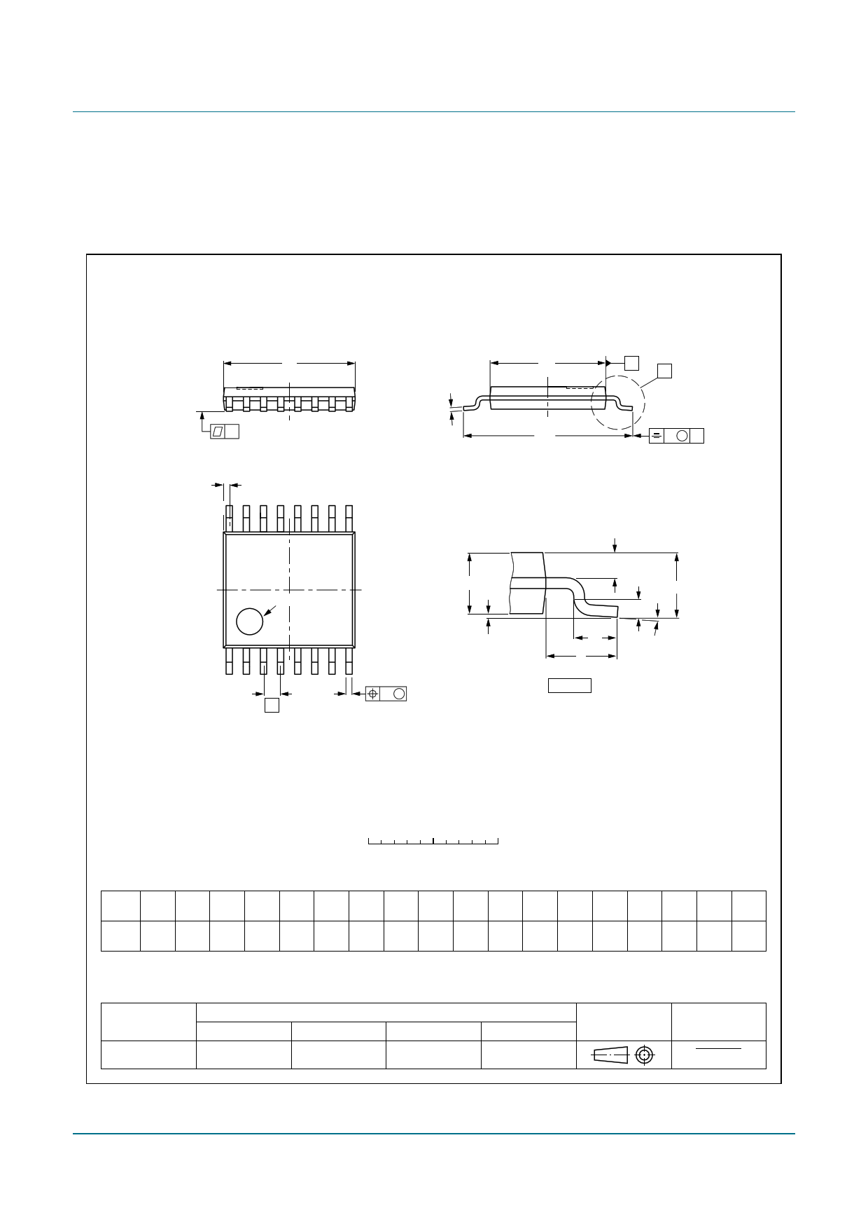
TSSOP16: plastic thin shrink small outline package; 16 leads; body width 4.4 mm
SOT403-1
D
y
Z
16
9
c
EA
X
HE v M A
pin 1 index
1
e
8
wM
bp
A2
A1
Q
(A3)
A
Lp
L
detail X
θ
0 2.5 5 mm
scale
DIMENSIONS (mm are the original dimensions)
UNIT
A
max.
A1
A2
A3
bp
c
mm
1.1
0.15
0.05
0.95
0.80
0.25
0.30
0.19
0.2
0.1
D (1) E (2)
e
5.1
4.9
4.5
4.3
0.65
HE
6.6
6.2
Notes
1. Plastic or metal protrusions of 0.15 mm maximum per side are not included.
2. Plastic interlead protrusions of 0.25 mm maximum per side are not included.
OUTLINE
VERSION
IEC
REFERENCES
JEDEC
JEITA
SOT403-1
MO-153
L Lp Q v w y Z (1) θ
1
0.75 0.4
0.50 0.3
0.2 0.13 0.1
0.40
0.06
8o
0o
EUROPEAN
PROJECTION
ISSUE DATE
99-12-27
03-02-18
Fig 13. Package outline SOT403-1 (TSSOP16)
NX5DV330_3
Product data sheet
Rev. 03 — 5 August 2009
© NXP B.V. 2009. All rights reserved.
11 of 15
11 Page | ||
| Páginas | Total 15 Páginas | |
| PDF Descargar | [ Datasheet NX5DV330.PDF ] | |
Hoja de datos destacado
| Número de pieza | Descripción | Fabricantes |
| NX5DV330 | Quad 1-of-2 video multiplexer/demultiplexer | NXP Semiconductors |
| Número de pieza | Descripción | Fabricantes |
| SLA6805M | High Voltage 3 phase Motor Driver IC. |
Sanken |
| SDC1742 | 12- and 14-Bit Hybrid Synchro / Resolver-to-Digital Converters. |
Analog Devices |
|
DataSheet.es es una pagina web que funciona como un repositorio de manuales o hoja de datos de muchos de los productos más populares, |
| DataSheet.es | 2020 | Privacy Policy | Contacto | Buscar |
