|
|
PDF TLE9260QXV33 Data sheet ( Hoja de datos )
| Número de pieza | TLE9260QXV33 | |
| Descripción | System Basis Chip | |
| Fabricantes | Infineon | |
| Logotipo |  |
|
Hay una vista previa y un enlace de descarga de TLE9260QXV33 (archivo pdf) en la parte inferior de esta página. Total 30 Páginas | ||
|
No Preview Available !
System Basis Chip
TLE9260QXV33
Mid-Range System Basis Chip Family
Body System IC with Integrated Voltage Regulators, Power Management Functions,
HS-CAN Transceiver supporting CAN FD .
Featuring Multiple High-Side Switches and High-Voltage Wake Inputs.
Data Sheet
Rev. 1.1, 2014-10-23
Automotive Power
1 page 
Mid-Range System Basis Chip Family
TLE9260QXV33
1 Overview
Scalable System Basis Chip Family
• Product family with various products for complete scalable application
coverage.
• Dedicated Data Sheets are available for the different product variants
• Complete compatibility (hardware and software) across the family
• TLE9263 with 2 LIN transceivers, 3 voltage regulators
• TLE9262 with 1 LIN transceiver, 3 voltage regulators
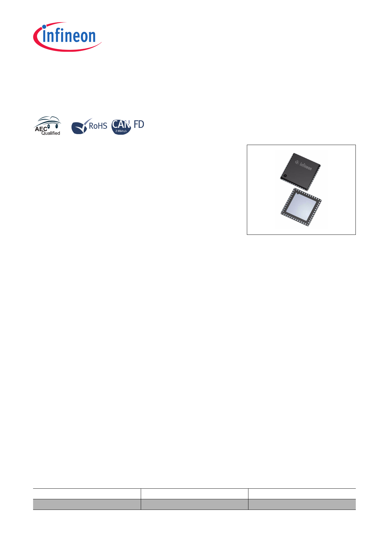
PG-VQFN-48-31
• TLE9261 without LIN transceivers, 3 voltage regulators
• TLE9260 without LIN transceivers, 2 voltage regulators
• Product variants for 5V (TLE926xQX) and 3.3V (TLE926xQXV33) output voltage for main voltage regulator
• CAN Partial Networking variants for 5V (TLE926x-3QX) and 3.3V (TLE926x-3QXV33) output voltage
Device Description
The TLE9260QXV33 is a monolithic integrated circuit in an exposed pad VQFN-48 (7mm x 7mm) power package
with Lead Tip Inspection (LTI) feature to support Automatic Optical Inspection (AOI).
The device is designed for various CAN automotive applications as main supply for the microcontroller and as
interface for a CAN bus network.
To support these applications, the System Basis Chip (SBC) provides the main functions, such as a 3.3V low-
dropout voltage regulator (LDO) for e.g. a microcontroller supply, another 5V low-dropout voltage regulator with
off-board protection for e.g. sensor supply , a HS-CAN transceiver supporting CAN FD for data transmission, high-
side switches with embedded protective functions and a 16-bit Serial Peripheral Interface (SPI) to control and
monitor the device. Also implemented are a configurable timeout / window watchdog circuit with a reset feature,
three Fail Outputs and an under voltage reset feature.
The device offers low-power modes in order to minimize current consumption on applications that are connected
permanently to the battery. A wake-up from the low-power mode is possible via a message on the buses, via the
bi-level sensitive monitoring/wake-up inputs as well as via cyclic wake.
The device is designed to withstand the severe conditions of automotive applications.
Type
TLE9260QXV33
Data Sheet
Package
PG-VQFN-48-31
5
Marking
TLE9260QXV33
Rev. 1.1, 2014-10-23
5 Page 
TLE9260QXV33
Pin Configuration
3.3 Hints for Unused Pins
It must be ensured that the correct configurations are also selected, i.e. in case functions are not used that they
are disabled via SPI:
• WK1/2/3: connect to GND and disable WK inputs via SPI
• HSx: leave open
• CANH/L, RXDCAN, TXDCAN: leave all pins open
• RO / FOx: leave open
• INT: leave open
• TEST: connect to GND during power-up to activate SBC Development Mode;
connect to VS or leave open for normal user mode operation
• VCC2: leave open and keep disabled
• VCAN: connect to VCC1
• n.c.: not connected; internally not bonded; connect to GND
• N.U.: Not Used; Used for internal testing purposes only. Do not connect, leave open, i.e. not connected to any
potential on the board. In case N.U. pins are connected on the board an open bridge has to be foreseen to
avoid external disturbances. The bridge can be shorted by a 0 Ω resistance if signal is needed.
3.4 Hints for Alternate Pin Functions
In case of alternate pin functions, selectable via SPI, it must be ensured that the correct configurations are also
selected via SPI, in case it is not done automatically. Please consult the respective chapter. In addition, following
topics shall be considered:
• WK1..2: The pins can be either used as HV wake / voltage monitoring inputs or for a voltage measurement
function (via bit WK_MEAS). In the second case, the WK1..2 pins shall not be used / assigned for any wake
detection nor cyclic sense functionality, i.e. WK1 and WK2 must be disabled in the register WK_CTRL_2 and
the level information is to be ignored in the register WK_LVL_STAT.
• FO2..3: The pins can also be configured as GPIOs in the GPIO_CTRL register. In this case, the pins shall not
be used for any fail output functionality. The default function after Power on Reset (POR) is FOx.
Data Sheet
11 Rev. 1.1, 2014-10-23
11 Page | ||
| Páginas | Total 30 Páginas | |
| PDF Descargar | [ Datasheet TLE9260QXV33.PDF ] | |
Hoja de datos destacado
| Número de pieza | Descripción | Fabricantes |
| TLE9260QXV33 | System Basis Chip | Infineon |
| Número de pieza | Descripción | Fabricantes |
| SLA6805M | High Voltage 3 phase Motor Driver IC. |
Sanken |
| SDC1742 | 12- and 14-Bit Hybrid Synchro / Resolver-to-Digital Converters. |
Analog Devices |
|
DataSheet.es es una pagina web que funciona como un repositorio de manuales o hoja de datos de muchos de los productos más populares, |
| DataSheet.es | 2020 | Privacy Policy | Contacto | Buscar |
