|
|
|
PDF ISL97649AR5566 Data sheet ( Hoja de datos )
| Número de pieza | ISL97649AR5566 | |
| Descripción | TFT-LCD Supply + DCP + VCOM Amplifier + Gate Pulse Modulator + RESET | |
| Fabricantes | Intersil | |
| Logotipo | ||
Hay una vista previa y un enlace de descarga de ISL97649AR5566 (archivo pdf) en la parte inferior de esta página. Total 21 Páginas | ||
|
No Preview Available !
DATASHEET
TFT-LCD Supply + DCP + VCOM Amplifier + Gate Pulse
Modulator + RESET
ISL97649AR5566
The ISL97649AR5566 is an Integrated Power Management IC
(PMIC) for TFT-LCDs used in notebooks, tablet PCs and monitors.
The device integrates a boost converter for generating AVDD, an
LDO for VLOGIC. VON and VOFF are generated by a charge pump
driven by the switch node of the boost. The ISL97649AR5566
also includes a VON slice circuit, reset function and a high
performance VCOM amplifier with DCP (Digitally Controlled
Potentiometer) that is used as a VCOM calibrator.
The AVDD boost converter features a 1.5A/0.18Ωboost FET with
600/1200kHz switching frequency.
The logic LDO includes a 350mA FET for driving the low voltage
needed by external digital circuitry.
The gate pulse modulator can control the gate voltage up to 30V,
and both the rate and slew delay times are selectable.
The supply monitor generates a reset signal when the system is
powered down.
It provides a programmable VCOM with I2C interface. One VCOM
amplifier is also integrated in the chip. The output of the VCOM is
powered up with the voltage at the last programmed 8-bit
EEPROM setting.
Features
• 2.5V to 5.5V input
• 1.5A, 0.18Ω integrated boost FET
• VON/VOFF supplies generated by charge pumps driven by the
boost switch node
• LDO for VLOGIC channel
• 600/1200kHz selectable switching frequency
• Integrated gate pulse modulator
• Reset signal generated by supply monitor
• Integrated VCOM amplifier
• DCP
- I2C serial interface, address: 0101000, MSB left
- Wiper position stored in 8-bit nonvolatile memory and
recalled on power-up
- Endurance, 1,000 data changes per bit
• UVLO, UVP, OVP, OCP and OTP protection
• Pb-free (RoHS compliant)
• 28 Ld 4x5 QFN
Applications
• LCD notebook, tablet and monitor
VIN
C1, 2
20µF
VIN
C32
0.1µF
VLOGIC
VLOGIC
LDO VIN
C25
1µF
C24
2.2µF
R18
3.92k
R17
8.25k
AVDD
C19
0.47µF
R9
10k
133k
R8
R7
83k
VCOM
September 11, 2015
FN8774.0
1
VIN
EN
SS
FREQ SEQUENCER
L_IN
AVDD BOOST
CONTROLLER
L1 10µH
LX
PGND
D1 C4, 5, 6
30µF
SW
R1
73.2k
AVDD
C7 AVDD
0.1µF
FB
COMP
R2 8.06k
R12 5.5k C20 15nF
D4
Q1
VOFF
L_OUT
ADJ
SCL
SDA
RSET
POS
AVDD
OUT
NEG
LDO
DCP
GPM
VCOM OP
VOLTAGE
DETECTOR
THERMAL PAD
VFLK
VGH
VDPM
CE
RE
VGHM
GPM_LO
VDIV
CD2
RESET
C11
0.1µF
AVDD
C15
1µF
C8
47nF
D2 C9
1µF
R6 1k
Z1
SW
C10
47nF
D3
C16
1µF
VON
C12
1µF
C17 1nF
C14 100pF
C28
0.1µF
R5 100k
C18
0.47µF
R14 85k
VGH GPM
R22 22k
R26 100k
VIN
OPEN
R15 115k
C26 1nF
RESET
AVDD
VGH
R16
10k
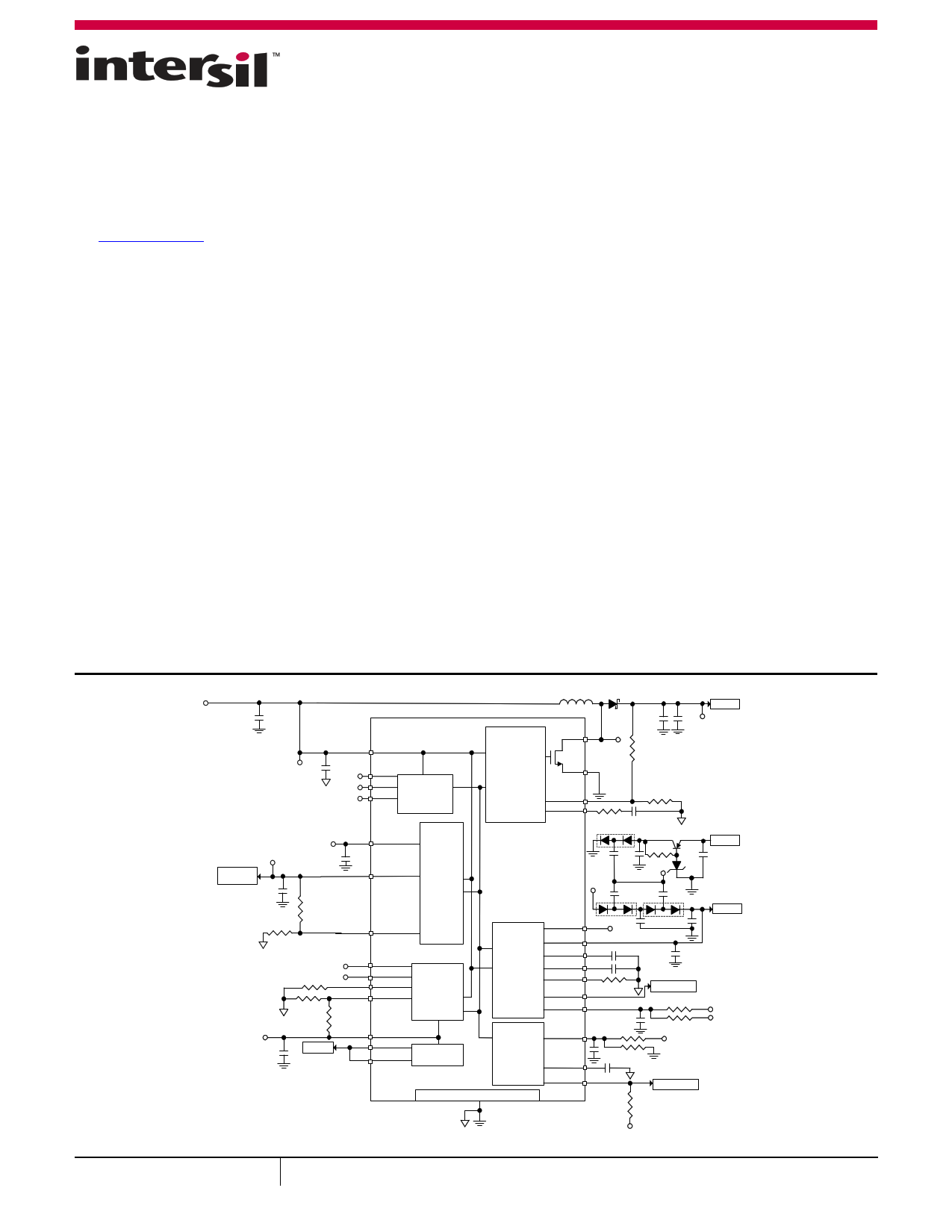
FIGURE 1. APPLICATION DIAGRAM
VLOGIC
CAUTION: These devices are sensitive to electrostatic discharge; follow proper IC Handling Procedures.
1-888-INTERSIL or 1-888-468-3774 | Copyright Intersil Americas LLC 2015. All Rights Reserved
Intersil (and design) is a trademark owned by Intersil Corporation or one of its subsidiaries.
All other trademarks mentioned are the property of their respective owners.
1 page 
ISL97649AR5566
Absolute Maximum Ratings
RE, VGHM, GPM_LO and VGH to GND . . . . . . . . . . . . . . . . . . . . -0.3 to +36V
LX, AVDD, POS, NEG, VOUT to GND. . . . . . . . . . . . . . . . . . . . . . . -0.3 to +18V
Voltage Between GND and PGND . . . . . . . . . . . . . . . . . . . . . . . . . . . . . ±0.5V
All Other Pins to GND . . . . . . . . . . . . . . . . . . . . . . . . . . . . . . . . -0.3 to +6.0V
ESD Rating
Human Body Model (Tested per JESD22-A114E) . . . . . . . . . . . . . . . . 2kV
Machine Model (Tested per JESD22-A115-A) . . . . . . . . . . . . . . . . . 200V
Charged Device Model (Tested per JESD22-C101). . . . . . . . . . . . . . . 1kV
Thermal Information
Thermal Resistance (Typical)
JA (°C/W) JC (°C/W)
28 Ld 4x5 QFN Package (Notes 4, 5). . . . .
38
4.5
Ambient Temperature . . . . . . . . . . . . . . . . . . . . . . . . . . . . . . -40°C to +85°C
Functional Junction Temperature . . . . . . . . . . . . . . . . . . . .-40°C to +150°C
Storage Temperature . . . . . . . . . . . . . . . . . . . . . . . . . . . . . .-65°C to +150°C
Lead Temperature During Soldering . . . . . . . . . . . . . . . . . . . . . . . . +260°C
Pb-free Reflow Profile . . . . . . . . . . . . . . . . . . . . . . . . . . . . . . . . . . see TB493
Recommended Operating Conditions
Temperature . . . . . . . . . . . . . . . . . . . . . . . . . . . . . . . . . . . . . . -40°C to +85°C
Supply Voltage . . . . . . . . . . . . . . . . . . . . . . . . . . . . . . . . . . . . . . . 2.5V to 5.5V
CAUTION: Do not operate at or near the maximum ratings listed for extended periods of time. Exposure to such conditions may adversely impact product
reliability and result in failures not covered by warranty.
NOTES:
4. JA is measured in free air with the component mounted on a high effective thermal conductivity test board with “direct attach” features. See Tech
Brief TB379.
5. For JC, the “case temp” location is the center of the exposed metal pad on the package underside.
Electrical Specifications VIN = ENABLE = 3.3V, AVDD = 8V, VLDO = 2.5V, VON = 24V, VOFF = - 6V. Boldface limits apply across the
operating temperature range, -40°C to +85°C.
SYMBOL
PARAMETER
TEST CONDITIONS
MIN TYP MAX
(Note 6) (Note 7) (Note 6) UNIT
GENERAL
VIN VIN Supply Voltage Range
IS_DIS
VIN Supply Currents when Disabled
VIN < UVLO
IS VIN Supply Currents
ENABLE = 3.3V, overdrive AVDD and VGH
IEBABLE
ENABLE Pin Current
ENABLE = 0V
LOGIC INPUT CHARACTERISTICS - ENABLE, FLK, SCL, SDA, FREQ
2.5 3.3 5.5 V
390 500 µA
0.7 1.0 mA
0 µA
VIL Low Voltage Threshold
VIH High Voltage Threshold
RIL Pull-Down Resistor
INTERNAL OSCILLATOR
Enable, FLK, FREQ
1.75
0.85
1.25
0.65
1.65
V
V
MΩ
FOSC
Switching Frequencies
AVDD BOOST REGULATOR
FREQ = low, TA = +25°C
FREQ = high, TA = +25°C
550
1100
600
1200
650
1300
kHz
kHz
DAVDD/
DIOUT
AVDD Load Regulation
50mA < ILOAD < 250mA
0.2 %
DAVDD/
DVIN
AVDD Line Regulation
ILOAD = 150mA, 2.5V < VIN < 5.5V
0.15
%
VFB
IFB
rDS(ON)
ILIM
DMAX
EFF
Feedback Voltage (VFB)
FB Input Bias Current
Switch ON-resistance
Switch Current Limit
Max Duty Cycle
LDO REGULATOR
ILOAD = 100mA, TA = +25°C
TA = +25°C
FREQ = 1.2MHz
FREQ = 1.2MHz, IAVDD = 100mA
0.792
0.8
0.808
V
100 nA
180 230 mΩ
1.125
1.5
1.875
A
80 90
%
91 %
DVLDO/
DVIN
Line Regulation
ILDO = 1mA, 3.0V < VIN1 < 5.5V
1 mV/V
Submit Document Feedback
5
FN8774.0
September 11, 2015
5 Page 
ISL97649AR5566
Applications Information
Enable Control
With VIN > UVLO, only the Logic output channel is activated. All
other functions in ISL97649AR5566 are shut down when the
enable pin is pulled down. When the voltage at the enable pin
reaches H threshold, the whole chip turns on.
Frequency Selection
The ISL97649AR5566 switching frequency can be user selected
to operate at either constant 600kHz or 1.2MHz. Lower switching
frequency can save power dissipation at very light load
conditions. Also, low switching frequency more easily leads to
discontinuous conduction mode, while higher switching
frequency allows for smaller external components, such as
inductor and output capacitors, etc. Higher switching frequency
will get higher efficiency within some loading range depending
on VIN, VOUT and external components, as shown in Figure 3 on
page 9. Connecting the FREQ pin to GND sets the PWM switching
frequency to 600kHz, or connecting FREQ pin to VIN for 1.2MHz.
Soft-Start
The soft-start is provided by an internal current source to charge
the external soft-start capacitor. The ISL97649AR5566 ramps up
the current limit from 0A up to the full value, as the voltage at the
SS pin ramps from 0V to 0.8V. Hence, the soft-start time is 3.2ms
when the soft-start capacitor is 22nF, 6.8ms for 47nF and
14.5ms for 100nF.
Operation
The boost converter is a current mode PWM converter operating
at either 600kHz or 1.2MHz. It can operate in both Discontinuous
Conduction Mode (DCM) at light load and Continuous Conduction
Mode (CCM). In continuous conduction mode, current flows
continuously in the inductor during the entire switching cycle in
steady state operation. The voltage conversion ratio in
continuous current mode is given by Equation 1:
V-----BV----oI--N-o---s---t = 1-----–-1----D---
(EQ. 1)
Where D is the duty cycle of the switching MOSFET.
The boost regulator uses a summing amplifier architecture
consisting of gm stages for voltage feedback, current feedback
and slope compensation. A comparator looks at the peak
inductor current cycle-by-cycle and terminates the PWM cycle if
the current limit is reached.
An external resistor divider is required to divide the output
voltage down to the nominal reference voltage. Current drawn by
the resistor network should be limited to maintain the overall
converter efficiency. The maximum value of the resistor network
is limited by the feedback input bias current and the potential for
noise being coupled into the feedback pin. A resistor network in
the order of 60kΩ is recommended. The boost converter output
voltage is determined by Equation 2:
VBoost = R-----1--R---+--2--R-----2- VFB
(EQ. 2)
The current through the MOSFET is limited to 1.5APEAK.
This restricts the maximum output current (average) based on
Equation 3:
IOMAX = ILMT – ---2--I--L- V-V----I-O-N--
(EQ. 3)
Where IL is the peak-to-peak inductor ripple current, and is set
by Equation 4:
IL = -V---L-I--N-- -f-S--D--W----
(EQ. 4)
where fSW is the switching frequency (600kHz or 1.2MHz).
Capacitor
An input capacitor is used to suppress the voltage ripple injected
into the boost converter. The ceramic capacitor with a
capacitance larger than 10µF is recommended. The voltage
rating of the input capacitor should be larger than the maximum
input voltage. Some input capacitors are recommended in
Table 1.
TABLE 1. BOOST CONVERTER INPUT CAPACITOR RECOMMENDATION
CAPACITOR
SIZE MFG
PART NUMBER
10µF/6.3V
0603 TDK
C1608X5R0J106M
10µF/16V
1206 TDK
C3216X7R1C106M
10µF/10V
0805 Murata
GRM21BR61A106K
22µF/10V
1210 Murata
GRB32ER61A226K
Inductor
The boost inductor is a critical part that influences the output
voltage ripple, transient response, and efficiency. Values of
3.3µH to 10µH are used to match the internal slope
compensation. The inductor must be able to handle the following
average and peak currents shown in Equation 5:
ILAVG
ILPK =
= 1----I-–-O----D---
ILAVG
+
---2--I--L-
(EQ. 5)
Some inductors are recommended in Table 2 for different design
considerations.
TABLE 2. BOOST CONVERTER INDUCTOR RECOMMENDATION
DIMENSIONS
INDUCTOR (mm)
MFG
PART
NUMBER
NOTE
10µH/ 8.3x8.3x4.5 Sumida CDR8D43-100NC
4Apeak
Efficiency
Optimization
6.8µH/ 5.0x5.0x2.0 TDK PLF5020T-6R8M1R8
1.8Apeak
10µH/ 6.6x7.3x1.2 Cyntec PCME061B-100MS
2.2Apeak
PCB
space/profile
optimization
Submit Document Feedback 11
FN8774.0
September 11, 2015
11 Page | ||
| Páginas | Total 21 Páginas | |
| PDF Descargar | [ Datasheet ISL97649AR5566.PDF ] | |
Hoja de datos destacado
| Número de pieza | Descripción | Fabricantes |
| ISL97649AR5566 | TFT-LCD Supply + DCP + VCOM Amplifier + Gate Pulse Modulator + RESET | Intersil |
| Número de pieza | Descripción | Fabricantes |
| SLA6805M | High Voltage 3 phase Motor Driver IC. |
Sanken |
| SDC1742 | 12- and 14-Bit Hybrid Synchro / Resolver-to-Digital Converters. |
Analog Devices |
|
DataSheet.es es una pagina web que funciona como un repositorio de manuales o hoja de datos de muchos de los productos más populares, |
| DataSheet.es | 2020 | Privacy Policy | Contacto | Buscar |