|
|
|
PDF MGA-43013 Data sheet ( Hoja de datos )
| Número de pieza | MGA-43013 | |
| Descripción | High Linearity 728 - 756MHz Power Amplifier Module | |
| Fabricantes | AVAGO | |
| Logotipo | ||
Hay una vista previa y un enlace de descarga de MGA-43013 (archivo pdf) en la parte inferior de esta página. Total 14 Páginas | ||
|
No Preview Available !
MGA-43013
High Linearity 728 - 756 MHz Power Amplifier Module
Data Sheet
Description
Avago Technologies’ MGA-43013 is a fully matched
power amplifier for use in the (728 – 756) MHz band.
High linear output power at 5 V is achieved through the
use of Avago Technologies’ proprietary 0.25 µm GaAs En-
hancement-mode pHEMT process. MGA-43013 is housed
in a miniature 5.0 mm × 5.0 mm molded chip-on-board
(MCOB) module package. A detector is also included
on-chip. The compact footprint coupled with high gain,
high linearity and good efficiency, makes the MGA-43013
an ideal choice as a power amplifier for small cell BTS PA
applications.
Applications
• Final stage high linearity amplifier for Picocell and
Enterprise Femtocell PA targeted for small cell BTS
downlink applications.
Component Image
AVAGO
43013
YYWW
XXXX
5.0 × 5.0 × 0.9 mm Package Outline
Notes:
Package marking provides orientation
and identification
”43013” = Device part number
”YYWW” = Year and work week
”XXXX” = Assembly lot number
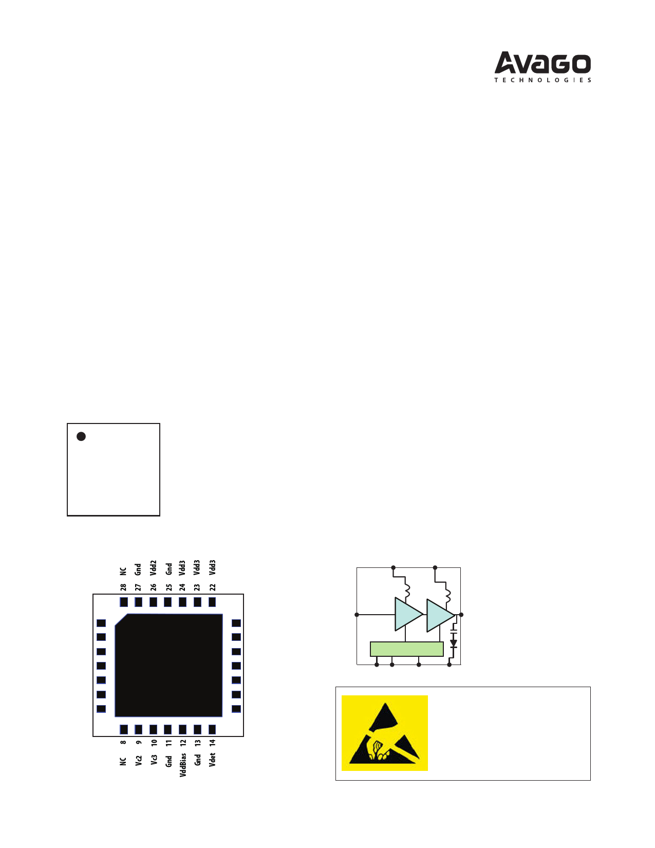
TOP VIEW
Pin Configuration
Features
• High linearity performance: Typ. -48 dBc ACLR1 [1] at 25
dBm linear output power (biased with 5 V supply)
• High Gain: 33.1 dB
• Good efficiency
• Fully matched
• Built-in detector
• GaAs E-pHEMT Technology [2]
• Low-cost small package size: (5.0 × 5.0 × 0.9) mm
• MSL3
• Lead-free/Halogen-free/RoHS compliance
Specifications
751 MHz; 5.0 V, Idqtotal = 270 mA (typ), LTE DL 10MHz 50
RB ETM 1.1 downlink signal
• PAE : 12.4%
• 25 dBm linear Pout @ ACLR1 = -48 dBc [1]
• 33.1 dB Gain
• Detector range : 20 dB
Notes:
1. LTE DL 10 MHz 50 RB ETM 1.1
2. Enhancement mode technology employs positive VGS, thereby
eliminating the need of negative gate voltage associated with
conventional depletion mode devices.
Functional Block Diagram
Vdd2 Vdd3
Gnd 1
Gnd 2
NC 3
RFin 4
NC 5
Gnd 6
NC 7
(5.0 × 5.0 × 0.9) mm
21 Gnd
20 Gnd
19 RFout
18 RFout
17 RFout
16 Gnd
15 Gnd
TOP VIEW
RFin
2nd Stage 3rd Stage
RFout
Biasing Circuit
Vc2 Vc3 VddBias Vdet
Attention: Observe precautions for
handling electrostatic sensitive devices.
ESD Machine Model = 60 V
ESD Human Body Model = 400 V
Refer to Avago Application Note A004R:
Electrostatic Discharge, Damage and Control.
1 page 
MGA-43013 typical over-temperature performance at Vc2 = 3 V, Vc3 = 2.6 V (Vdd = VddBias = 5 V) as shown in
Figure 20 unless otherwise stated
-10
2fo_85ºC 2fo_25°C 2fo_-40°C
37.0
Gain_85°C
Gain_25°C
2600
-15
3fo_85°C
3fo_25°C
3fo_-40°C
Gain_-40°C
Idd_Total_85ºC
-20
35.0
Idd_Total_-40ºC
Idd_Total_25ºC
2200
-25 33.0 1800
-30
-35 31.0 1400
-40 29.0 1000
-45
27.0 600
-50
-55
728 730 732 734 736 738 740 742 744 746 748 750 752 754 756
Frequency/MHz
Figure 12. Over-temperature 2nd, 3rd Harmonics vs Freq at Pout=25dBm,
Vdd=VddBias=5.0V operating voltage
25.0 200
22 23 24 25 26 27 28 29 30 31 32 33 34 35 36 37 38
Pout/dBm
Figure 13. Over-temperature Gain, Idd_Total vs Pout @ 733MHz,
Vdd=VddBias=5.0V operating voltage
37.0
Gain_85°C
Gain_25°C
Gain_-40°C
2600
Idd_Total_85ºC Idd_Total_25ºC Idd_Total_-40ºC
35.0 2200
33.0 1800
31.0 1400
29.0 1000
27.0 600
25.0 200
22 23 24 25 26 27 28 29 30 31 32 33 34 35 36 37 38
Pout/dBm
Figure 14. Over-temperature Gain, Idd_Total vs Pout @ 739MHz,
Vdd=VddBias=5.0V voltage
37.0 2600
35.0 2200
33.0 1800
31.0 1400
29.0 1000
27.0 600
Gain_85°C
Gain_25°C
Gain_-40°C
Idd_Total_85ºC Idd_Total_25ºC Idd_Total_-40ºC
25.0 200
22 23 24 25 26 27 28 29 30 31 32 33 34 35 36 37 38
Pout/dBm
Figure 15. Over-temperature Gain, Idd_Total vs Pout @ 751MHz,
Vdd=VddBias=5.0V operating voltage
5
5 Page 
MGA-43013 typical Ic2, Ic3 vs. Vc performance, unless otherwise stated
Vc /V
Figure 22. Ic vs. Vc at Vdd = VddBias = 5.0 V
PCB Land Pattern and Stencil Outline
5.00
3.60
0.45
Pin1
5.00
0.40
0.75
0.60
∅0.30
0.25
1.25 3.70
0.05
0.80
0.68
0.50
4.77
0.23
0.50 1.13 0.82
3.24
1.52
Soldermask
Opening
0.50
(pitch)
Land Pattern
0.25
Soldermask
0.27
0.50
Stencil Opening
5.00
3.60
3.24
0.45
1.82
1.13 4.77
0.68
0.80
Top Metal
3.60 5.00
Notes:
1. Recommended Land Pattern and Stencil
2. 4 mils stencil thickness recommended
3. All dimensions are in mm
0.05
Combination of Land Pattern & Stencil Opening
11
11 Page | ||
| Páginas | Total 14 Páginas | |
| PDF Descargar | [ Datasheet MGA-43013.PDF ] | |
Hoja de datos destacado
| Número de pieza | Descripción | Fabricantes |
| MGA-43013 | High Linearity 728 - 756MHz Power Amplifier Module | AVAGO |
| Número de pieza | Descripción | Fabricantes |
| SLA6805M | High Voltage 3 phase Motor Driver IC. |
Sanken |
| SDC1742 | 12- and 14-Bit Hybrid Synchro / Resolver-to-Digital Converters. |
Analog Devices |
|
DataSheet.es es una pagina web que funciona como un repositorio de manuales o hoja de datos de muchos de los productos más populares, |
| DataSheet.es | 2020 | Privacy Policy | Contacto | Buscar |