|
|
|
PDF LTC2422 Data sheet ( Hoja de datos )
| Número de pieza | LTC2422 | |
| Descripción | 1-/2-Channel 20-Bit uPower No Latency ADCs | |
| Fabricantes | Linear | |
| Logotipo | ||
Hay una vista previa y un enlace de descarga de LTC2422 (archivo pdf) en la parte inferior de esta página. Total 30 Páginas | ||
|
No Preview Available !
LTC2421/LTC2422
1-/2-Channel 20-Bit µPower
No Latency ∆ΣTMADCs in MSOP-10
FEATURES
DESCRIPTIO
s 20-Bit ADCs in Tiny MSOP-10 Packages
s 1- or 2-Channel Inputs
s Single Supply 2.7V to 5.5V Operation
s Low Supply Current (200µA) and Auto Shutdown
s Automatic Channel Selection (Ping-Pong) (LTC2422)
s No Latency: Digital Filter Settles in a
Single Conversion Cycle
s 8ppm INL, No Missing Codes
s 4ppm Full-Scale Error
s 0.5ppm Offset
s 1.2ppm Noise
s Zero Scale and Full Scale Set for Reference
and Ground Sensing
s Internal Oscillator—No External Components Required
s 110dB Min, 50Hz/60Hz Notch Filter
s Reference Input Voltage: 0.1V to VCC
s Live Zero—Extended Input Range Accommodates
12.5% Overrange and Underrange
s Pin Compatible with LTC2401/LTC2402
U
APPLICATIO S
s Weight Scales
s Direct Temperature Measurement
s Gas Analyzers
s Strain Gauge Transducers
s Instrumentation
s Data Acquisition
s Industrial Process Control
The LTC®2421/LTC2422 are 1- and 2-channel 2.7V to 5.5V
micropower 20-bit analog-to-digital converters with an
integrated oscillator, 8ppm INL and 1.2ppm RMS noise.
These ultrasmall devices use delta-sigma technology and
a new digital filter architecture that settles in a single cycle.
This eliminates the latency found in conventional ∆Σ
converters and simplifies multiplexed applications.
Through a single pin, the LTC2421/LTC2422 can be
configured for better than 110dB rejection at 50Hz or
60Hz ±2%, or can be driven by an external oscillator for
a user defined rejection frequency in the range 1Hz to
120Hz. The internal oscillator requires no external fre-
quency setting components.
These converters accept an external reference voltage
from 0.1V to VCC. With an extended input conversion
range of –12.5% VREF to 112.5% VREF (VREF = FSSET –
ZSSET), the LTC2421/LTC2422 smoothly resolve the off-
set and overrange problems of preceding sensors or
signal conditioning circuits.
The LTC2421/LTC2422 communicate through a 2- or
3-wire digital interface that is compatible with SPI and
MICROWIRETM protocols.
, LTC and LT are registered trademarks of Linear Technology Corporation.
No Latency ∆Σ is a trademark of Linear Technology Corporation.
MICROWIRE is a trademark of National Semiconductor Corporation.
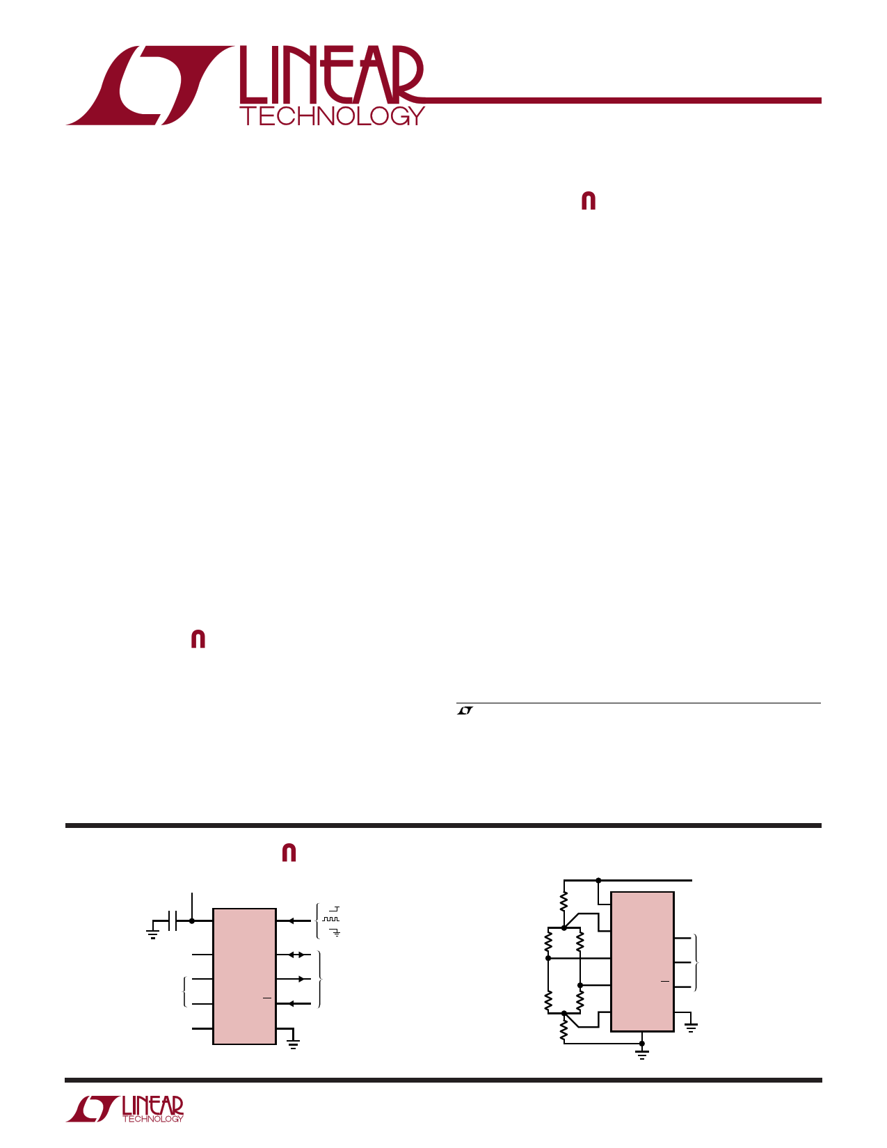
TYPICAL APPLICATIO
2.7V TO 5.5V
1µF
REFERENCE VOLTAGE
ZSSET + 0.1V TO VCC
ANALOG INPUT RANGE
ZSSET – 0.12VREF TO
FSSET + 0.12VREF
(VREF = FSSET – ZSSET)
0V TO FSSET – 100mV
1
VCC
10
FO
LTC2422
2
FSSET
9
SCK
3
CH1
SDO 8
4
CH0
CS 7
56
ZSSET GND
VCC
= INTERNAL OSC/50Hz REJECTION
= EXTERNAL CLOCK SOURCE
= INTERNAL OSC/60Hz REJECTION
3-WIRE
SPI INTERFACE
24212 TA01
Pseudo Differential Bridge Digitizer
1
VCC
2 LTC2422
FSSET SCK 9
4
CH0
SDO 8
3
CH1
7
CS
2.7V TO 5.5V
3-WIRE
SPI INTERFACE
5
ZSSET
GND
6
10
FO
INTERNAL OSCILLATOR
60Hz REJECTION
24012TA02
24212f
1
1 page 
TYPICAL PERFOR A CE CHARACTERISTICS
LTC2421/LTC2422
Total Unadjusted Error (3V Supply)
10
VCC = 3V
8 VREF = 2.5V
6
4
2
0
–2
–4
–6 TA = –55°C, –45°C, 25°C, 90°C
–8
–10
0
0.5 1.0 1.5 2.0
INPUT VOLTAGE (V)
2.5
24212 G01
Positive Extended Input Range
Total Unadjusted Error (3V Supply)
10
VCC = 3V
8 VREF = 2.5V
6
4
2
0
–2
–4
–6 TA = –55°C, –45°C, 25°C, 90°C
–8
–10
2.50 2.55 2.60 2.65 2.70 2.75 2.80
INPUT VOLTAGE (V)
24212 G04
Negative Extended Input Range
Total Unadjusted Error (5V Supply)
10
VCC = 5V
8 VREF = 5V
6
4
2
TA = 25°C
TA = 90°C
TA = –45°C
TA = –55°C
0
–2
–4
–6
–8
–10
0
–0.05 –0.10 –0.15 –0.20 –0.25 –0.30
INPUT VOLTAGE (V)
24212 G07
INL (3V Supply)
10
VCC = 3V
8 VREF = 2.5V
6
4
2
0
–2
–4
TA = –55°C, –45°C, 25°C, 90°C
–6
–8
–10
0
0.5 1.0 1.5 2.0
INPUT VOLTAGE (V)
2.5
24212 G02
Total Unadjusted Error (5V Supply)
10
VCC = 5V
8 VREF = 5V
6
4
2
0
–2
–4
TA = –55°C, –45°C, 25°C, 90°C
–6
–8
–10
0
1 2 34
INPUT VOLTAGE (V)
5
24212 G05
Positive Extended Input Range
Total Unadjusted Error (5V Supply)
10
VCC = 5V
8 VREF = 5V
6
4
2
0
–2
–4
TA = –55°C
–6
–8 TA = 90°C TA = 25°C
TA = –45°C
–10
5.00 5.05 5.10 5.15 5.20 5.25 5.30
INPUT VOLTAGE (V)
24212 G08
Negative Extended Input Range
Total Unadjusted Error (3V Supply)
10
VCC = 3V
8 VREF = 2.5V
6
TA = 90°C
TA = 25°C
4 TA = –45°C
2
0
–2 TA = –55°C
–4
–6
–8
–10
0
–0.05 –0.10 –0.15 –0.20 –0.25 –0.30
INPUT VOLTAGE (V)
24212 G03
INL (5V Supply)
10
VCC = 5V
8 VREF = 5V
6
4
2
0
–2
–4
TA = –55°C, –45°C, 25°C, 90°C
–6
–8
–10
0
1 2 34
INPUT VOLTAGE (V)
5
24212 G06
Offset Error vs Reference Voltage
150
VCC = 5V
TA = 25°C
120
90
60
30
0
01 2 345
REFERENCE VOLTAGE (V)
24212 G09
24212f
5
5 Page 
LTC2421/LTC2422
APPLICATIO S I FOR ATIO
Conversion Clock
A major advantage delta-sigma converters offer over con-
ventional type converters is an on-chip digital filter (com-
monly known as Sinc or Comb filter). For high resolution,
low frequency applications, this filter is typically designed
to reject line frequencies of 50Hz or 60Hz plus their har-
monics. In order to reject these frequencies in excess of
110dB, a highly accurate conversion clock is required. The
LTC2421/LTC2422 incorporate an on-chip highly accu-
rate oscillator. This eliminates the need for external fre-
quency setting components such as crystals or oscilla-
tors. Clocked by the on-chip oscillator, the LTC2421/
LTC2422 reject line frequencies (50Hz or 60Hz ±2%) a
minimum of 110dB.
Ease of Use
The LTC2421/LTC2422 data output has no latency, filter
settling or redundant data associated with the conver-
sion cycle. There is a one-to-one correspondence be-
tween the conversion and the output data. Therefore,
multiplexing an analog input voltage is easy.
The LTC2421/LTC2422 perform offset and full-scale cali-
brations every conversion cycle. This calibration is trans-
parent to the user and has no effect on the cyclic operation
described above. The advantage of continuous calibration
is extreme stability of offset and full-scale readings with
respect to time, supply voltage change and temperature
drift.
Power-Up Sequence
The LTC2421/LTC2422 automatically enter an internal reset
state when the power supply voltage VCC drops below
approximately 2.2V. This feature guarantees the integrity
of the conversion result and of the serial interface mode
selection which is performed at the initial power-up. (See
the 2-wire I/O sections in the Serial Interface Timing Modes
section.)
When the VCC voltage rises above this critical threshold,
the converter creates an internal power-on-reset (POR)
signal with duration of approximately 0.5ms. The POR
signal clears all internal registers. Following the POR sig-
nal, the LTC2421/LTC2422 start a normal conversion cycle
and follows the normal succession of states described
above. The first conversion result following POR is accu-
rate within the specifications of the device.
Reference Voltage Range
The LTC2421/LTC2422 can accept a reference voltage(VREF
= FSSET – ZSSET) from 0V to VCC. The converter output
noise is determined by the thermal noise of the front-end
circuits, and as such, its value in microvolts is nearly con-
stant with reference voltage. A decrease in reference volt-
age will not significantly improve the converter’s effective
resolution. On the other hand, a reduced reference voltage
will improve the overall converter INL performance. The
recommended range for the LTC2421/LTC2422 voltage
reference is 100mV to VCC.
Input Voltage Range
The converter is able to accommodate system level offset
and gain errors as well as system level overrange situa-
tions due to its extended input range, see Figure 3. The
LTC2421/LTC2422 convert input signals within the ex-
tended input range of – 0.125 • VREF to 1.125 • VREF
(VREF = FSSET – ZSSET).
For large values of VREF (VREF = FSSET – ZSSET), this range
is limited by the absolute maximum voltage range of
– 0.3V to (VCC + 0.3V). Beyond this range, the input ESD
protection devices begin to turn on and the errors due to
the input leakage current increase rapidly.
Input signals applied to VIN may extend below ground by
– 300mV and above VCC by 300mV. In order to limit any
VCC + 0.3V
FSSET + 0.12VREF
FSSET
NORMAL
INPUT
RANGE
EXTENDED
INPUT
RANGE
ABSOLUTE
MAXIMUM
INPUT
RANGE
ZSSET
ZSSET – 0.12VREF
–0.3V
(VREF = FSSET – ZSSET)
24212 F03
Figure 3. LTC2421/LTC2422 Input Range
24212f
11
11 Page | ||
| Páginas | Total 30 Páginas | |
| PDF Descargar | [ Datasheet LTC2422.PDF ] | |
Hoja de datos destacado
| Número de pieza | Descripción | Fabricantes |
| LTC2420 | 20-Bit uPower No Latency ADC in SO-8 | Linear Technology |
| LTC2420C | 20-Bit uPower No Latency ADC in SO-8 | Linear Technology |
| LTC2420CS8 | 20-Bit uPower No Latency ADC in SO-8 | Linear Technology |
| LTC2420I | 20-Bit uPower No Latency ADC in SO-8 | Linear Technology |
| Número de pieza | Descripción | Fabricantes |
| SLA6805M | High Voltage 3 phase Motor Driver IC. |
Sanken |
| SDC1742 | 12- and 14-Bit Hybrid Synchro / Resolver-to-Digital Converters. |
Analog Devices |
|
DataSheet.es es una pagina web que funciona como un repositorio de manuales o hoja de datos de muchos de los productos más populares, |
| DataSheet.es | 2020 | Privacy Policy | Contacto | Buscar |