|
|
|
PDF ADG5249F Data sheet ( Hoja de datos )
| Número de pieza | ADG5249F | |
| Descripción | 8:1/Dual 4:1 Multiplexers | |
| Fabricantes | Analog Devices | |
| Logotipo | ||
Hay una vista previa y un enlace de descarga de ADG5249F (archivo pdf) en la parte inferior de esta página. Total 30 Páginas | ||
|
No Preview Available !
Data Sheet
User Defined Fault Protection and
Detection, 0.8 pC QINJ, 8:1/Dual 4:1 Multiplexers
ADG5248F/ADG5249F
FEATURES
User defined secondary supplies set overvoltage level
Overvoltage protection up to −55 V and +55 V
Power-off protection up to −55 V and +55 V
Overvoltage detection on source pins
Minimum secondary supply level: 4.5 V single-supply
Interrupt flags indicate fault status
Low charge injection (QINJ): 0.8 pC
Low drain/source on capacitance
ADG5248F: 19 pF
ADG5249F: 14 pF
Latch-up immune under any circumstance
Known state without digital inputs present
VSS to VDD analog signal range
±5 V to ±22 V dual supply operation
8 V to 44 V single-supply operation
Fully specified at ±15 V, ±20 V, +12 V, and +36 V
APPLICATIONS
Analog input/output modules
Process control/distributed control systems
Data acquisition
Instrumentation
Avionics
Automatic test equipment
Communication systems
Relay replacement
GENERAL DESCRIPTION
The ADG5248F and ADG5249F are 8:1 and dual 4:1 analog
multiplexers. The ADG5248F switches one of eight inputs to a
common output, and the ADG5249F switches one of four differen-
tial inputs to a common differential output. Each channel conducts
equally well in both directions when on, and each channel has an
input signal range that extends to the supplies. The primary supply
voltages define the on-resistance profile, whereas the secondary
supply voltages define the voltage level at which the overvoltage
protection engages.
When no power supplies are present, the channel remains in the off
condition, and the switch inputs are high impedance. Under normal
operating conditions, if the analog input signal levels on any Sx pin
exceed positive fault voltage (POSFV) or negative fault voltage
(NEGFV) by a threshold voltage (VT), the channel turns off and
that Sx pin becomes high impedance. If the switch on, the drain pin
is pulled to the secondary supply voltage that was exceeded. Input
signal levels up to +55 V or −55 V relative to ground are blocked, in
both the powered and unpowered conditions.
Rev. 0
Document Feedback
Information furnished by Analog Devices is believed to be accurate and reliable. However, no
responsibility is assumed by Analog Devices for its use, nor for any infringements of patents or other
rights of third parties that may result from its use. Specifications subject to change without notice. No
license is granted by implication or otherwise under any patent or patent rights of Analog Devices.
Trademarksandregisteredtrademarksarethepropertyoftheirrespectiveowners.
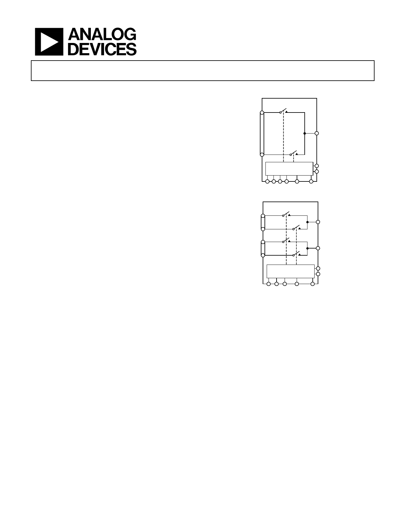
FUNCTIONAL BLOCK DIAGRAMS
ADG5248F
S1
D
S8
FAULT DETECTION
AND
SWITCH DRIVER
FF
SF
A0 A1 A2 EN POSFV NEGFV
Figure 1. ADG5248F Functional Block Diagram
ADG5249F
S1A
S4A
DA
S1B
S4B
DB
FAULT DETECTION
AND
SWITCH DRIVER
FF
SF
A0 A1 EN POSFV NEGFV
Figure 2. ADG5249F Functional Block Diagram
The low capacitance and charge injection of these switches make
them ideal solutions for data acquisition and sample-and-hold
applications, where low glitch switching and fast settling times
are required.
Note that, throughout this data sheet, multifunction pins, such as
A0/F0, are referred to either by the entire pin name or by a single
function of the pin, for example, A0, when only that function is
relevant.
PRODUCT HIGHLIGHTS
1. Source pins are protected against voltages greater than the
secondary supply rails, up to −55 V and +55 V.
2. Source pins are protected against voltages between −55 V
and +55 V in an unpowered state.
3. Overvoltage detection with digital output indicates
operating state of switches.
4. Trench isolation guards against latch-up.
5. Optimized for low charge injection and on capacitance.
6. The ADG5248F/ADG5249F can be operated from a dual
supply of ±5 V to ±22 V or a single power supply of 8 V to 44 V.
One Technology Way, P.O. Box 9106, Norwood, MA 02062-9106, U.S.A.
Tel: 781.329.4700
©2015 Analog Devices, Inc. All rights reserved.
Technical Support
www.analog.com
1 page 
Data Sheet
ADG5248F/ADG5249F
Parameter
Fault Mode
IDD
IPOSFV
IDD + IPOSFV
IGND
ISS
INEGFV
ISS + INEGFV
VDD/VSS
+25°C
1.4
0.2
2.2
0.9
1.6
0.45
0.2
1.0
−40°C to
+85°C
−40°C to
+125°C
2.3
1.7
1.1
±5
±22
Unit
mA typ
mA typ
mA max
mA typ
mA max
mA typ
mA typ
mA max
V min
V max
Test Conditions/Comments
VS = ±55 V
GND = 0 V
GND = 0 V
1 Guaranteed by design; not subject to production test.
±20 V DUAL SUPPLY
VDD = 20 V ± 10%, VSS = −20 V ± 10%, GND = 0 V, CDECOUPLING = 0.1 µF, unless otherwise noted.
Table 2.
Parameter
ANALOG SWITCH
Analog Signal Range
On Resistance, RON
On-Resistance Match Between
Channels, ∆RON
On-Resistance Flatness, RFLAT(ON)
Threshold Voltage, VT
LEAKAGE CURRENTS
Source Off Leakage, IS (Off )
Drain Off Leakage, ID (Off )
Channel On Leakage, ID (On), IS (On)
FAULT
Source Leakage Current, IS
With Overvoltage
−40°C to −40°C to
+25°C +85°C +125°C Unit
260
280 345
250
270 335
2.5
6 12
2.5
6 12
12.5
14 15
1.5
3.5 4
0.7
VDD to VSS
405
395
V
Ω typ
Ω max
Ω typ
Ω max
Ω typ
13 Ω max
Ω typ
13 Ω max
Ω typ
15 Ω max
Ω typ
4 Ω max
V typ
±0.1
±1 ±2
±0.1
±1 ±5
±0.3
±1.5 ±20
±5
±10
±25
nA typ
nA max
nA typ
nA max
nA typ
nA max
±66 µA typ
Power Supplies Grounded or Floating ±25
µA typ
Test Conditions/Comments
VDD = +18 V, VSS = −18 V, see Figure 36
VS = ±15 V, IS = −1 mA
VS = ±13.5 V, IS = −1 mA
VS = ±15 V, IS = −1 mA
VS = ±13.5 V, IS = −1 mA
VS = ±15 V, IS = −1 mA
VS = ±13.5 V, IS = −1 mA
See Figure 28
VDD = +22 V, VSS = −22 V
VS = ±15 V, VD = ∓15 V, see Figure 34
VS = ±15 V, VD = ∓15 V, see Figure 34
VS = VD = ±15 V, see Figure 35
VDD = 22 V, VSS = −22 V, GND = 0 V, VS = ±55 V,
see Figure 33
VDD = 0 V or floating, VSS = 0 V or floating, GND =
0 V, Ax = 0 V or floating, VS = ±55 V, see Figure 32
Rev. 0 | Page 5 of 33
5 Page 
Data Sheet
ADG5248F/ADG5249F
Parameter
Charge Injection, QINJ
Off Isolation
Channel-to-Channel Crosstalk
Adjacent Channels
Nonadjacent Channels
Total Harmonic Distortion Plus Noise,
THD + N
−3 dB Bandwidth
ADG5248F
ADG5249F
Insertion Loss
CS (Off )
CD (Off )
ADG5248F
ADG5249F
CD (On), CS (On)
ADG5248F
ADG5249F
POWER REQUIREMENTS
Normal Mode
IDD
IPOSFV
IDD + IPOSFV
IGND
ISS
INEGFV
ISS + INEGFV
Fault Mode
IDD
IPOSFV
IDD + IPOSFV
IGND
ISS
INEGFV
ISS + INEGFV
VDD
+25°C
−1.2
−75
−40°C to
+85°C
−75
−88
0.007
200
320
10.5
4
13
7
18
12
1.15
0.15
2
0.75
1.4
0.3
0.2
0.65
1.4
0.2
2.2
0.9
1.6
0.45
0.2
1.0
1 Guaranteed by design; not subject to production test.
−40°C to
+125°C
2
1.4
0.7
2.3
1.7
1.1
8
44
Unit
pC typ
dB typ
dB typ
dB typ
% typ
MHz typ
MHz typ
dB typ
pF typ
pF typ
pF typ
pF typ
pF typ
mA typ
mA typ
mA max
mA typ
mA max
mA typ
mA typ
mA max
mA typ
mA typ
mA max
mA typ
mA max
mA typ
mA typ
mA max
V min
V max
Test Conditions/Comments
VS = 18 V, RS = 0 Ω, CL = 1 nF, see Figure 49
RL = 50 Ω, CL = 5 pF, f = 1 MHz, see Figure 39,
worst case channel
RL = 50 Ω, CL = 5 pF, f = 1 MHz, see Figure 38
RL = 10 kΩ, VS = 18 V p-p, f = 20 Hz to 20 kHz,
see Figure 37
RL = 50 Ω, CL = 5 pF, see Figure 40
RL = 50 Ω, CL = 5 pF, f = 1 MHz, see Figure 40
VS = 18 V, f = 1 MHz
VS = 18 V, f = 1 MHz
VS = 18 V, f = 1 MHz
VDD = 39.6 V; VSS = 0 V; digital inputs = 0 V, 5 V, or VDD
VS = +55 V, −40 V
GND = 0 V
GND = 0 V
Rev. 0 | Page 11 of 33
11 Page | ||
| Páginas | Total 30 Páginas | |
| PDF Descargar | [ Datasheet ADG5249F.PDF ] | |
Hoja de datos destacado
| Número de pieza | Descripción | Fabricantes |
| ADG5249F | 8:1/Dual 4:1 Multiplexers | Analog Devices |
| Número de pieza | Descripción | Fabricantes |
| SLA6805M | High Voltage 3 phase Motor Driver IC. |
Sanken |
| SDC1742 | 12- and 14-Bit Hybrid Synchro / Resolver-to-Digital Converters. |
Analog Devices |
|
DataSheet.es es una pagina web que funciona como un repositorio de manuales o hoja de datos de muchos de los productos más populares, |
| DataSheet.es | 2020 | Privacy Policy | Contacto | Buscar |