|
|
|
PDF LT3991-3.3 Data sheet ( Hoja de datos )
| Número de pieza | LT3991-3.3 | |
| Descripción | 1.2A Step-Down Regulator | |
| Fabricantes | Linear | |
| Logotipo | ||
Hay una vista previa y un enlace de descarga de LT3991-3.3 (archivo pdf) en la parte inferior de esta página. Total 24 Páginas | ||
|
No Preview Available !
Features
n Ultralow Quiescent Current:
2.8µA IQ Regulating 12VIN to 3.3VOUT
n Fixed Output Voltages: 3.3V, 5V
2.1µA IQ Regulating 12VIN
n Low Ripple Burst Mode® Operation:
Output Ripple < 15mVP-P
n Wide Input Voltage Range: 4.3V to 55V
n 1.2A Maximum Output Current
n Adjustable Switching Frequency: 200kHz to 2MHz
n Synchronizable Between 250kHz to 2MHz
n Fast Transient Response
n Accurate 1V Enable Pin Threshold
n Low Shutdown Current: IQ = 700nA
n Power Good Flag
n Soft-Start CapabilityV
n Internal Compensation
n Saturating Switch Design: 0.44Ω On-Resistance
n Output Voltage: 1.19V to 30V
n Small Thermally Enhanced 10-Pin MSOP Package
and (3mm × 3mm) DFN Packages
Applications
n Automotive Battery Regulation
n Power for Portable Products
n Industrial Supplies
LT3991/LT3991-3.3/LT3991-5
55V, 1.2A Step-Down
Regulator with 2.8µA
Quiescent Current
Description
The LT®3991 is an adjustable frequency monolithic buck
switching regulator that accepts a wide input voltage range
up to 55V. Low quiescent current design consumes only
2.8µA of supply current while regulating with no load. Low
ripple Burst Mode operation maintains high efficiency at
low output currents while keeping the output ripple below
15mV in a typical application. An internally compensated
current mode topology is used for fast transient response
and good loop stability. A high efficiency 0.44Ω switch
is included on the die along with a boost Schottky diode
and the necessary oscillator, control and logic circuitry.
An accurate 1V threshold enable pin can be used to shut
down the LT3991, reducing the input supply current to
700nA. A capacitor on the SS pin provides a controlled
inrush current (soft-start). A power good flag signals
when VOUT reaches 91% of the programmed output volt-
age. The LT3991 is available in small 10-pin MSOP and
3mm × 3mm DFN packages with exposed pads for low
thermal resistance.
L, LT, LTC, LTM, Burst Mode, Linear Technology and the Linear logo are registered trademarks
of Linear Technology Corporation. All other trademarks are the property of their respective
owners.
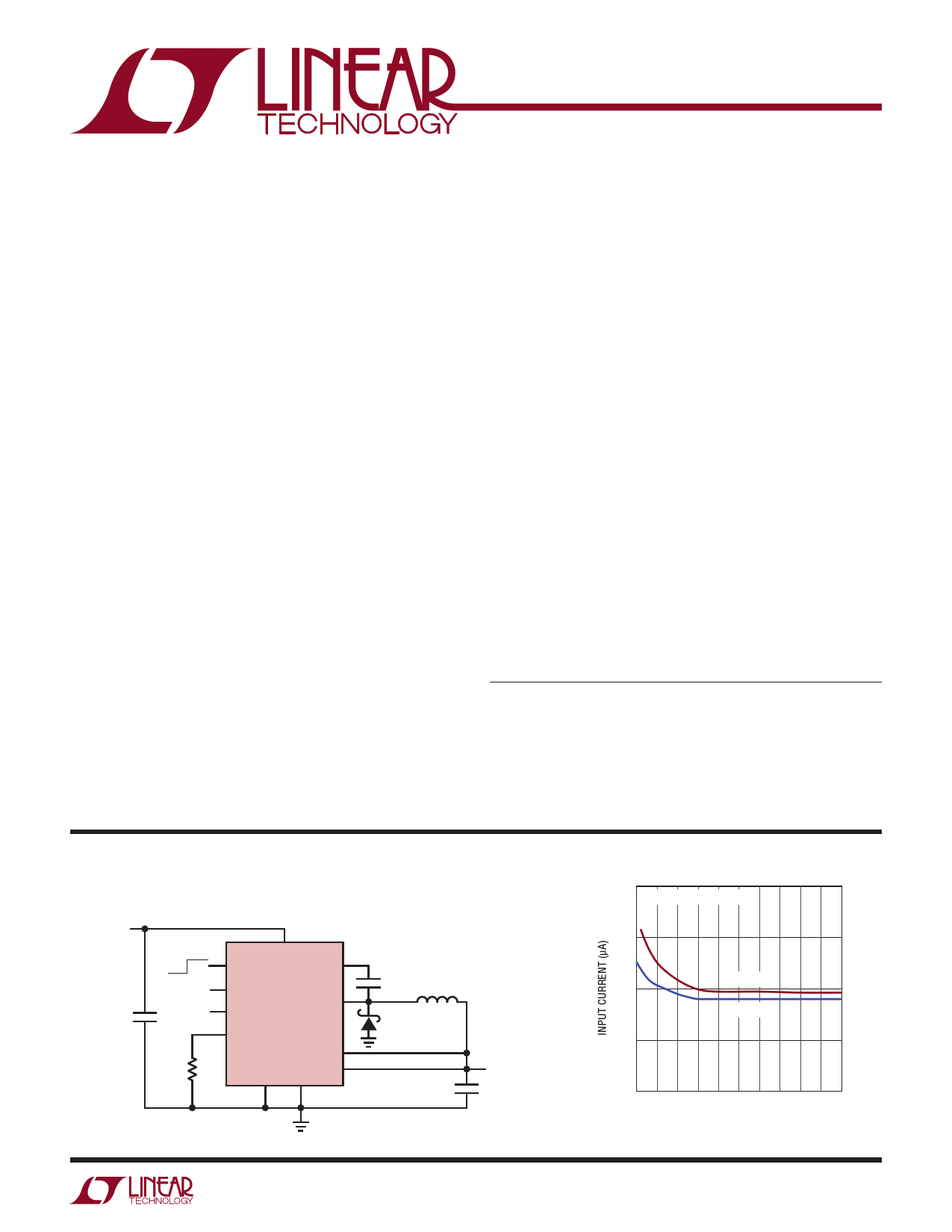
Typical Application
VIN
4.3V TO 55V
3.3V Step Down Converter
OFF ON
VIN
EN./UVLO
BOOST
4.7µF
PG
SS LT3991-3.3 SW
118k
RT
SYNC
BD
GND VOUT
0.47µF 12µH
47µF
f = 400kHz
3991 TA01a
VOUT
3.3V
1.2A
No Load Supply Current
3.0
OUTPUT IN REGULATION
2.5
LT3991-5
2.0
LT3991-3.3
1.5
1.0
5
10 15 20 25 30 35 40 45 50 55
INPUT VOLTAGE (V)
3991 G06
3991fa
1
1 page 
LT3991/LT3991-3.3/LT3991-5
Typical Performance Characteristics TA = 25°C, unless otherwise noted.
Maximum Load Current
3.0 VOUT = 3.3V
2.5
2.0 TYPICAL
1.5 MINIMUM
1.0
0.5
0
5 10 15 20 25 30 35 40 45 50 55
INPUT VOLTAGE (V)
3991 G08
Switching Frequency
1000
950
900
850
800
750
700
650
600
–55 –25
5 35 65 95
TEMPERATURE (°C)
125 155
3991 G11
Switch VCESAT
700
600
500
400
300
200
100
0
0 250 500 750 1000 1250 1500
SWITCH CURRENT (mA)
3991 G14
Maximum Load Current
2.5 VOUT = 5V
2.0
TYPICAL
1.5
MINIMUM
1.0
0.5
0
5 10 15 20 25 30 35 40 45 50 55
INPUT VOLTAGE (V)
3991 G09
Switch Current Limit
3.0
2.5
2.0
1.5
1.0
0.5
0
0 20 40 60 80 100
DUTY CYCLE (%)
3991 G12
Boost Pin Current
45
40
35
30
25
20
15
10
5
0
0 250 500 750 1000 1250 1500
SWITCH CURRENT (mA)
3991 G15
Load Regulation
0.30
0.25 REFERENCED FROM VOUT AT 0.5A LOAD
0.20
0.15
0.10
0.05
0
–0.05
–0.10
–0.15
–0.20
–0.25
–0.30
0
200 400 600 800 1000 1200
LOAD CURRENT (mA)
3991 G10
Switch Current Limit
2.5
2.4
2.3
2.2
2.1
2.0
1.9
1.8
1.7
1.6
DUTY CYCLE = 30%
1.5
–55 –25 5 35 65 95
TEMPERATURE (°C)
125 155
3991 G13
LT3991 Frequency Foldback
900
800
700
600
500
400
300
200
100
0
0 0.2 0.4 0.6 0.8 1 1.2
FB PIN VOLTAGE (V)
3991 G16
3991fa
5
5 Page 
LT3991/LT3991-3.3/LT3991-5
Applications Information
Operating Frequency Tradeoffs
Selection of the operating frequency is a tradeoff between
efficiency, component size, minimum dropout voltage, and
maximum input voltage. The advantage of high frequency
operation is that smaller inductor and capacitor values may
be used. The disadvantages are lower efficiency, lower
maximum input voltage, and higher dropout voltage. The
highest acceptable switching frequency (fSW(MAX)) for a
given application can be calculated as follows:
fSW (MAX )
=
VOUT
tON(MIN)(VIN
+ VD
− VSW
+
VD )
where VIN is the typical input voltage, VOUT is the output
voltage, VD is the catch diode drop (~0.5V), and VSW is
the internal switch drop (~0.5V at max load). This equation
shows that slower switching frequency is necessary to
safely accommodate high VIN/VOUT ratio. Also, as shown
in the Input Voltage Range section, lower frequency allows
a lower dropout voltage. The input voltage range depends
on the switching frequency because the LT3991 switch has
finite minimum on and off times. The minimum switch on
and off times are strong functions of temperature. Use
the typical minimum on and off curves to design for an
application’s maximum temperature, while adding about
30% for part-to-part variation. The minimum and maximum
duty cycles that can be achieved taking minimum on and
off times into account are:
DCMIN = fSW tON(MIN)
DCMAX = 1− fSW tOFF(MIN)
where fSW is the switching frequency, the tON(MIN) is the
minimum switch on-time, and the tOFF(MIN) is the minimum
switch off-time. These equations show that duty cycle
range increases when switching frequency is decreased.
See the Electrical Characteristics section for tON(MIN) and
tOFF(MIN) values.
A good choice of switching frequency should allow ad-
equate input voltage range (see Input Voltage Range sec-
tion) and keep the inductor and capacitor values small.
Input Voltage Range
The minimum input voltage is determined by either the
LT3991’s minimum operating voltage of 4.3V or by its
maximum duty cycle (see equation in Operating Frequency
Tradeoffs section). The minimum input voltage due to
duty cycle is:
VIN(MIN)
=
VOUT + VD
1− fSW tOFF(MIN)
−
VD
+
VSW
where VIN(MIN) is the minimum input voltage, VOUT is
the output voltage, VD is the catch diode drop (~0.5V),
VSW is the internal switch drop (~0.5V at max load), fSW
is the switching frequency (set by RT), and tOFF(MIN) is
the minimum switch off-time. Note that higher switch-
ing frequency will increase the minimum input voltage.
If a lower dropout voltage is desired, a lower switching
frequency should be used.
The maximum input voltage for LT3991 applications
depends on switching frequency, the Absolute Maximum
Ratings of the VIN and BOOST pins, and the operating
mode. For a given application where the switching fre-
quency and the output voltage are already selected, the
maximum input voltage (VIN(OP-MAX)) that guarantees
optimum output voltage ripple for that application can be
found by applying the following equation:
VIN(OP -MAX )
=
VOUT + VD
fSW • tON(MIN)
–
VD
+ VSW
where tON(MIN) is the minimum switch on-time. Note that
a higher switching frequency will decrease the maximum
operating input voltage. Conversely, a lower switching
frequency will be necessary to achieve normal operation
at higher input voltages.
The circuit will tolerate inputs above the maximum op-
erating input voltage and up to the Absolute Maximum
Ratings of the VIN and BOOST pins, regardless of chosen
switching frequency. However, during such transients
where VIN is higher than VIN(OP-MAX), the LT3991 will enter
pulse-skipping operation where some switching pulses are
skipped to maintain output regulation. The output voltage
ripple and inductor current ripple will be higher than in
typical operation. Do not overload when VIN is greater
than VIN(OP-MAX).
3991fa
11
11 Page | ||
| Páginas | Total 24 Páginas | |
| PDF Descargar | [ Datasheet LT3991-3.3.PDF ] | |
Hoja de datos destacado
| Número de pieza | Descripción | Fabricantes |
| LT3991-3.3 | 1.2A Step-Down Regulator | Linear |
| Número de pieza | Descripción | Fabricantes |
| SLA6805M | High Voltage 3 phase Motor Driver IC. |
Sanken |
| SDC1742 | 12- and 14-Bit Hybrid Synchro / Resolver-to-Digital Converters. |
Analog Devices |
|
DataSheet.es es una pagina web que funciona como un repositorio de manuales o hoja de datos de muchos de los productos más populares, |
| DataSheet.es | 2020 | Privacy Policy | Contacto | Buscar |