|
|
|
PDF L9822E Data sheet ( Hoja de datos )
| Número de pieza | L9822E | |
| Descripción | OCTAL SERIAL SOLENOID DRIVER | |
| Fabricantes | STMicroelectronics | |
| Logotipo | ||
Hay una vista previa y un enlace de descarga de L9822E (archivo pdf) en la parte inferior de esta página. Total 11 Páginas | ||
|
No Preview Available !
L9822E
OCTAL SERIAL SOLENOID DRIVER
. EIGHT LOW RDSon DMOS OUTPUTS
(0.5Ω AT IO = 1A @ 25°C VCC = 5V± 5%)
. 8 BIT SERIAL INPUT DATA (SPI)
. 8 BIT SERIAL DIAGNOSTIC OUTPUT FOR
OVERLOADAND OPENCIRCUIT CONDITIONS
. OUTPUT SHORT CIRCUIT PROTECTION
. CHIPENABLESELECTFUNCTION (active low)
. INTERNAL 36V CLAMPING FOR EACH OUT-
PUT
. CASCADABLE WITH ANOTHER OCTAL
DRIVER
. LOW QUIESCENT CURRENT (10mA MAX.)
. PACKAGE MULTIWATT15, PowerSO20 AND
SO20L
DESCRIPTION
The L9822E is an octal low side solenoid driver
rea lized in Multipower-BCD technology particularly
suited for driving lamps, relays and solenoids in au-
ADVANCE DATA
MULTIPOWER BCD TECHNOLOGY
PowerSO20 SO20L (16+2+2) Multiwatt15
ORDERING NUMBERS: L9822E (Multiwatt15)
L9822EPD (Power SO20)
L9822ED (SO20L )
tomotive environment. The DMOS outpts L9822E
has a very low power consumption.
Data is transmitted serially to the device using the
Serial Peripheral Interface (SPI) protocol.
The L9822E features the outputs status monitoring
function.
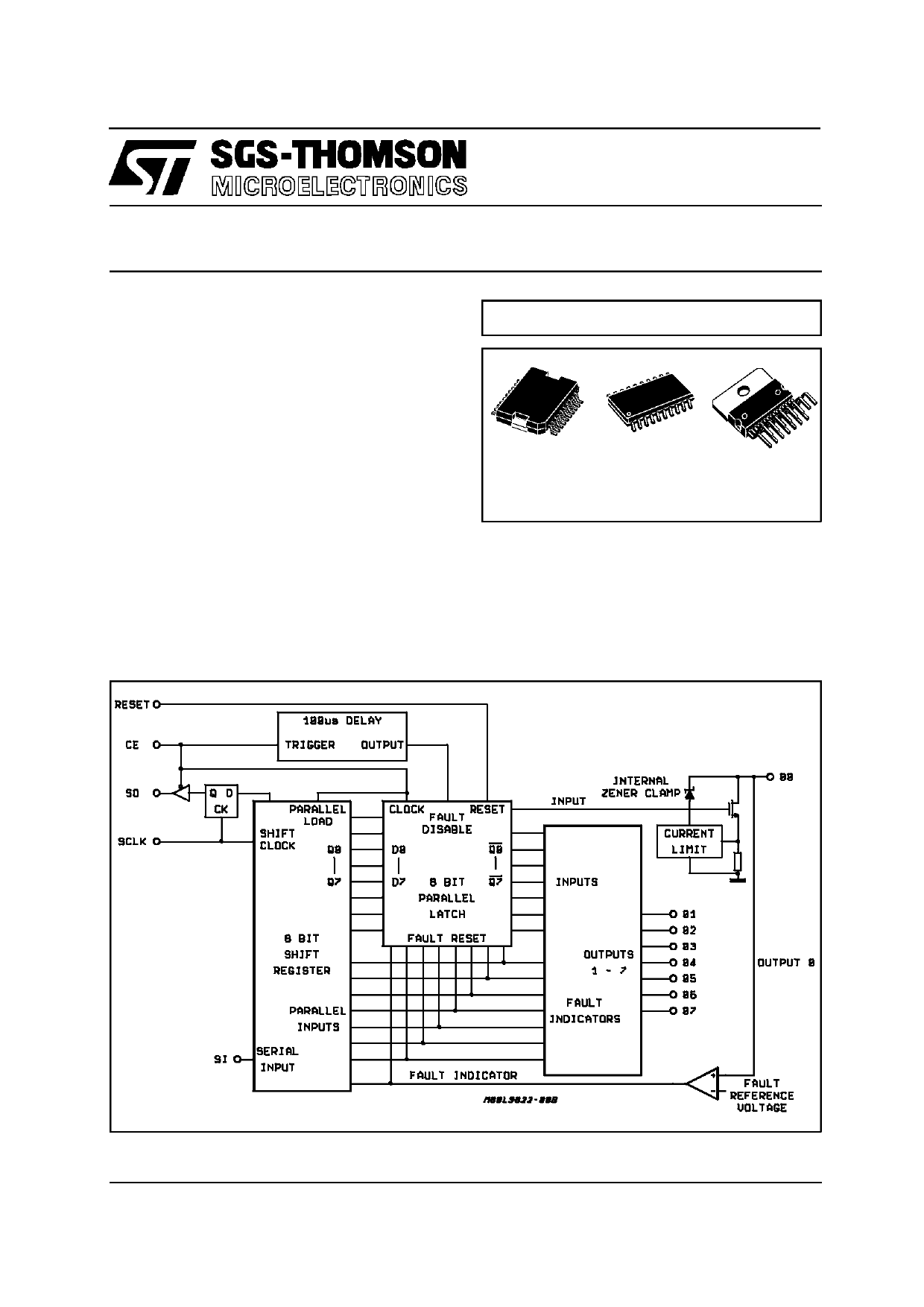
BLOCK DIAGRAM
September 1994
1/11
This is advanced information on a new product now in development or undergoing evaluation. Details are subject to change without notice.
1 page 
L9822E
FUNCTIONAL DESCRIPTION
The L9822ESP DMOS output is a low operating po-
wer device featu-ring,eight 1Ω RDSON DMOSdrivers
with transient protection circuits in output stages.
Each channel is independentlycontrolled by an out-
put latch and a common RESET line which disables
all eight outputs. The driver has low saturation and
shortcircuit protectionand candrive inductiveandre-
sistive loads such as solenoids, lamps and relais.
Datais transmittedtothe deviceseriallyusingtheSe-
rialPeripheral Interface(SPI) protocol. The circuit re-
ceives 8 bit serial data by means of the serial input
(SI) which is stored in an internal register to control
the output drivers. The serial output (SO) provides 8
bit of diagnostic data representing the voltage level
at the driver output. This allows the microprocessor
to diagnosethe condition of the output drivers.
The output saturation voltage is monitored by a
comparator for an out of saturation condition and is
able to unlatch the particular driver through the fault
reset line. This circuit is also cascadable with ano-
ther octal driver in order to jam 8 bit multiple data.
The device is selected when the chip enable (CE)
line is low.
Additionally the (SO) is placed in a tri-state mode
when the device is deselected. The negative edge
of the (CE) transfers the voltage level of the drivers
to the shift registerand the positive edge of the (CE)
latchesthe new datafrom the shift registerto the dri-
vers. When CE is Low, data bit contained into the
shift register is transferred to SO output at every
SCLK positive transition while data bit present at SI
input is latched into the shift register on every SCLK
negative transition.
Internal Blocks Description
The internal architecture of the device is based on
the three internal major blocks : the octal shift regi-
ster for talking to the SPI bus, the octal latch for hol-
ding control bits written into the device and the octal
load driver array.
Shift Register
The shift register has both serial and parallel inputs
and serial and parallel outputs. The serial input ac-
cepts data from the SPI bus and the serial output si-
multaneously sends data into the SPI bus. The
parallel outputs are latched into the parallel latch in-
side the L9822ESPat the end of adata transfer. The
parallel inputs jam diagnostic data into the shift re-
gister at the beginning of a data transfer cycle.
Parallel Latch
The parallel latch holds the input data from the shift
register. This data then actuates the output stages.
Individual registers in the latch may be cleared by
fault conditions in order to protect the overloaded
output stages. The entire latch may also be cleared
by the RESET signal.
Output Stages
The output stagesprovide an active low drive signal
suitable for 0.75A continuous loads. Each output
has a current limit circuit which limits the maximum
output current to at least 1.05A to allow for high in-
rush currents. Additionally,the outputshaveinternal
zeners set to 36 volts to clamp inductive transients
at turn-off. Each output also has a voltage compa-
rator observing the outputnode. If the voltage exce-
eds 1.8V on an ON output pin, a fault condition is
assumed and the latch driving this particular stage
is reset, turning the output OFF to protect it. The ti-
ming of this action is described below. These com-
parators also provide diagnostic feedback data to
the shift register. Additionally, the comparatorscon-
tainan internalpulldowncurrentwhich will causethe
cell to indicate a low output voltage if the output is
programmedOFF and the output pin is open circui-
ted.
TIMING DATA TRANSFER
Figure #2 shows the overall timing diagram from a
byte transfer to and from the L9822ESP using the
SPI bus.
CE High to Low Transition
The action begins when the Chip Enable(CE) pin is
pulledlow. The tri-state Serial Output(SO)pin driver
will be enabledentire time that CE is low. At the fal-
ling edge of the CE pin, the diagnostic data from the
voltage comparatorsin the output stages will be lat-
ched into the shift register. If a particular output is
high, a logic one will be jammed into that bit in the
shift register. If the output is low, a logic zero will be
loadedthere. The most significant bit (07) shouldbe
presented at the Serial Input (SI) pin. A zero at this
pin will program an output ON, while a one will pro-
gram the output OFF.
SCLK Transitions
The Serial Clock (SCLK) pin should then be pulled
high. At thispoint the diagnostic bit from the most si-
gnificantoutput(07) will appearat the SO pin.A high
here indicates that the 07 pin is higher than 1.8V.
The SCLK pin shouldthen be toggledlow then high.
New SO data will appearfollowingevery rising edge
of SCLK and new SI data will be latched into the
L9822ESPshift register on the falling edges. An un-
limited amount of data may be shifted through the
5/11
5 Page 
L9822E
Information furnished is believed to be accurate and reliable. However, SGS-THOMSON Microelectronics assumes no responsibility for
the consequences of use of such information nor for any infringement of patents or other rights of third parties which may result from its
use. No license is granted by implication or otherwise under any patent or patent rights of SGS-THOMSON Microelectronics. Specification
mentioned in this publication are subject to change without notice. This publication supersedes and replaces all information previously
supplied. SGS-THOMSON Microelectronics products are not authorized for use as critical components in life support devices or systems
without express written approval of SGS-THOMSON Microelectronics.
© 1996 SGS-THOMSON Microelectronics – Printed in Italy – All Rights Reserved
MULTIWATT® is a Registered Trademark of SGS-THOMSON Microelectronics
PowerSO-20™ is a Trademark of SGS-THOMSON Microelectronics
SGS-THOMSON Microelectronics GROUP OF COMPANIES
Australia - Brazil - Canada - China - France - Germany - Hong Kong - Italy - Japan - Korea - Malaysia - Malta - Morocco -
The Netherlands - Singapore - Spain - Sweden - Switzerland - Taiwan - Thailand - United Kingdom - U.S.A.
11/11
11 Page | ||
| Páginas | Total 11 Páginas | |
| PDF Descargar | [ Datasheet L9822E.PDF ] | |
Hoja de datos destacado
| Número de pieza | Descripción | Fabricantes |
| L9822E | OCTAL SERIAL SOLENOID DRIVER | STMicroelectronics |
| L9822ED | OCTAL SERIAL SOLENOID DRIVER | STMicroelectronics |
| L9822EPD | OCTAL SERIAL SOLENOID DRIVER | STMicroelectronics |
| L9822N | OCTAL SERIAL SOLENOID DRIVER | STMicroelectronics |
| Número de pieza | Descripción | Fabricantes |
| SLA6805M | High Voltage 3 phase Motor Driver IC. |
Sanken |
| SDC1742 | 12- and 14-Bit Hybrid Synchro / Resolver-to-Digital Converters. |
Analog Devices |
|
DataSheet.es es una pagina web que funciona como un repositorio de manuales o hoja de datos de muchos de los productos más populares, |
| DataSheet.es | 2020 | Privacy Policy | Contacto | Buscar |